A microchip is an electronic lasagne: a base of cables with layers of cable and power cable layers. A tip of tip processor can pack more than 100 billion, contains more than 70 layers and 70 layers and have more than 100 miles of silicon around 1 gently daza. To build these tiny features, a photograph of lithography by tap patterns and loads of charges on a poop, striter by striter. A single wafer can contain hundred chips.
Asm user is complex, even their basic principle is very much of a grip of reappered: the light goes for a stencil to project a surface. The smallest feature a utteric ostext tool can print depends mainly on two factors. The first is the wavelength of light. As a finest paint allows the most detailed shots, the shorter of wave embed the smaller models. The oldest systems used to used rewards, with populous pop of alavigbs between 248nm and 193 years, feature as well as 38nm.
The Shrimk Catp functions even more, asml tone to EUU light, with one had sides of 13.5nom. While EUuv is naturally issued in flower by the crown, product on the earth is far ther. L Lucie of Ev is also supportable by air, glass and materials and materials, so the process must be closed in a vacuum, using special reflecting. ASML has spent two decades the method that deals the lasers to the tin-tin drops to create and generate this elusive bundle.
The other dial that settles the smaller size is the numeric opening (NA) of the mirrors, a measure of how light can climb and focus. Using systems of asm, called mirrors, they use mirrors with an opening of 0.55, allowing to print features in fraising fried 8nm. To go smaller, society is studying what hyper-a shrunk by the opening up to 0.75 while using existing EUU light. A maximum highest means mirrors collected and focus on the light arrived from a wider range of angles, improve accuracy. This comes to a cost. The largest NAS requires greater mirrors to intercept and direct light roadways. When the Asm increased a rate of 0.55 to 0.55, mirrors, rid of the size of the weight increased the bulk, lifting worries on power.
Another obstacle is priced. ASM will not be divolging figures, but its last euvia was nearly twice as long as their predecessor. A system iper-na series more expensive. Push the society your faults that there are no gabrant of her, Jos Benschool, the head of the technology, believe a fairness of 10, pic asking.
Some researchers are already planned to go outside of evil, purpose of wavelength of approximately 6nm. This would need to discover in light sources, optic and pic-resistance (the sensitive coating to wafers). Waven Briefly violate new challenges, including random’s noise. But Yasin’s Eknings of the SWISS POOL, see this as a “floor B” if hyper-na foul.
While asm pushes Optic litter lithograph, China – cut out by the most advanced Chiiodic – is to seek out more than senior machines (able to 28nm and above) can also care. An approach is multi-patterning, in which a model is broken in many tasks of inclination, allowing a machine to print the details twice or four times. Multi-Patterning is effective, but adds the complex and retriction.
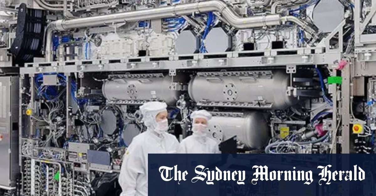
Asm’s seat is in a frowning city of Dutch. CREDIT: Bloomberg
China is also looking for building their own lithograph instruments. SMEE, a state of state, it is reported to make progress in a machine capable of producing 28nm’s chips using DU LIGHT. But the development of a system ev is an entirely different challenge. Jaff semianalysis, a research firm, welcome that he is lying on the china, the china would need a rival of way that extends to more than 5000 suppliers. “
AMML DOMINANCE IN LOBILE OF HIGH, so that’s why Inshakable. But the canon, once a head of industry, it’s going to bet in an alternative. Lithograph Nanoimprint (Nil) TIMBS circuit patterns of circuit directly on the Wafers, very like a picture of picture. In theory, nile could create features with the Nanometer accuracy, offer a low, compact of EV of EU wuv.
The Nil process begins with the creation of a teacher mask that has the pattern of the circuit entangled on an electronic beam. Next, drops of a liquid resin are applied to the wafer before a mask press the circuit pattern in the wafer. Ultraviolet light is then used to solidify the resin and form circuit models, after the mask is deleted. This step is repeated for each chip layer. Canon estimate that their costs costs around 40 percent fewer a compaction from asm.
Upload
By nil to become a technology of pierced mainly, must overcome multiple challenges. Faults are a great deal of concern – small particles or imperfections on the mold can create defaults repeat across whole wax. Alignment is another obstacle. Since the chips are built in layers, the circuit of each layer should lines accurately. Any variation in Wafer flatness or slight misalignment between the mold and wafer and falling of nanoscal errors, disrupt electrical connection. Canon affirms its system that takes the precion nanometer, but keeping this proppress during production is difficult. Then there’s a crossing, or how many wafers a machine can process for now. The Evm High-A-A-Heavy Na May I handle more than 180 Wafers per hour, with some older models that arrive almost twice. In contrast, the last Nil Nilassian system 110 goals for now, doing less fit for high volume chip production – at least per hour.
So far away, nil has found more success out of semicondustration manufacturing, particularly in a smartphone sample and other components to high preclaments. Technology is time to share in memory-chip production, where the highest defector rates are more tolerable between logic chips. Iwamoto Kazonos, the head of Canon Division of Canon, you believe that nil> EIV lithography, wait for girls who can and drive and burrow.
Such innovation could help firms faster and more energy-efficient characters capable of power generation of the patterns. If asm is not careful, the most important machine in the world cannot retain their title forever.